Four printable ESP32-S3 bench parts — three come as STL downloads, the fourth only as a browser generator
Three STL files you can download from this page. A bench plate that parks a half-size (BB400) solderless breadboard and an ESP32-S3-DevKitC-1 side by side, a fit gauge whose six stepped channels exist to measure the one dimension this repository could not source from an authority, and a jumper-wire comb whose teeth stand on the 2.54 mm breadboard pitch.
Read this before you download. These files have not been printed — not by me, not by anyone I know of. They are geometry that has been checked by code and by nothing else.
What was checked: twenty-six
assertions run against the finished solids by tools/print/test-fit.cjs, and an
independent re-read of the written STL bytes by tools/print/verify-stl.cjs. What
was not checked: a printer. There is no photo of any of them, no measured tolerance,
no material or print-time result, and no report from anyone who has used one. This page is a
download plus the method behind it. It is not a write-up of something that got made.
What you may do with all of this. Separately from whether the geometry is
any good, you are free to use it. The three STL files, the SVG outlines and anything the
browser generators on this page hand you are released under
CC BY 4.0; the generator
code behind them — the .cjs listings linked throughout this page — is
MIT.
So: remix a part, print it, sell the print, re-post it on Printables or anywhere else, without asking. The one thing asked in return is that you credit dankbuild.com with a link back to this page, link the licence alongside it, and say that you changed the file if you did.
Both licence files are plain text and open in the tab — LICENSE-CC-BY-4.0.txt carries an attribution line you can paste as it stands, and LICENSE-MIT.txt is the full MIT text. Permission is not a promise the part works: the paragraph above still stands.
You do not have to take the files as they are. All three parts can also be built in this tab, around a number of your own rather than the one this repository picked: see Make a plate sized to the numbers you measured, Re-centre the gauge on a number you already have and Build a comb with the number of teeth you want, further down.
You type a number, the same generator code that produced the STLs above runs in your browser, and it either hands you a file or refuses and says why. Nothing is uploaded and nothing is stored; if JavaScript is off, those controls simply never appear and the downloads are unaffected.
A fourth part has no file above it at all.
Build a tray for the loose parts on your bench is an open-top box
sized from an inside length and an inside width you type. There is no
bench-tray.stl to download, and that is deliberate: any size this page published
would be a guess about somebody else's bench, so the generator has no default and refuses,
in writing, until you give it both dimensions.
It is the same code path as the three above, and it has been printed exactly as often as they have, which is never.
Everything dimensional below is either a parameter you can read in
tools/print/models.cjs or a bounding box that came back from re-reading the
binary STL files that this page serves. Where a parameter is marked UNVERIFIED in the
generator, this page says so instead of quietly rounding it into a fact.
The bench plate
esp32-bench-plate.stl — 120.3 × 63.1 × 5.6 mm overall, 96 triangles, 4884 bytes. Two bays side by side on one slab, so tugging a jumper wire at one end does not drag the whole arrangement across the desk.
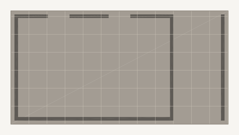
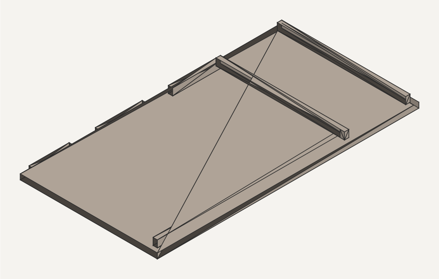
esp32-bench-plate.stl: the flat top view, and an isometric projection of the
same mesh. Both were written by
verify-stl.cjs
out of the STL bytes it had just re-read — they are renders, not photographs, and not
pictures of a print, because nothing has been printed. The isometric one shades each facet
by its normal so the form reads; the checker's own comment calls that view “genuinely
ambiguous about which walls exist and where the openings are”, which is why the top
view is still here next to it.- Breadboard bay — 84.1 × 55.1 mm. That is the BB400 footprint
of 83.5 × 54.5 mm in
models.cjsplus 0.6 mm of clearance for moulding draft. The half-size breadboard footprint follows from the 2.54 mm tie-point pitch rather than from any one vendor's tooling, which is whymodels.cjsis willing to state it: it is consistent across suppliers to a few tenths of a millimetre. - Devkit bay — 26.2 mm wide, and open at both ends. Only the width constrains anything. The front and rear walls stop at the divider, so a board longer than the plate simply overhangs at both ends instead of colliding with a wall.
- Two cable notches, 12.0 mm wide, cut into the rear wall over the breadboard half, so wires leave the plate rather than getting pinched under it.
- Walls 2.0 mm thick and 3.2 mm tall above a 2.4 mm base. That height retains parts without burying the pin rows you need to reach with a probe.
The fit gauge, and the number nobody could source
The header comment in models.cjs is blunt about the problem: the DevKitC-1's
board outline could not be obtained from an authority. That claim was re-checked on
2026-08-08 and it needed correcting.
The documentation URL those notes were built on does still return 404, but only because the guide was renamed to a versioned filename and the old path was left dead; the guide that replaced it resolves, and it links a public DXF dimensions source that resolves too. What the DXF does not contain is a dimension callout — it is vector geometry, not a table, so a width still has to be measured, in CAD or in plastic.
This site's hardest rule is that no hardware fact may be invented. So the width parameter stays marked UNVERIFIED in the generator, and the gauge exists to replace it with a reading.
The method behind that decision — how the sourcing check was actually run, why the bay is left open on the axis nobody could confirm, and what each layer of checking catches — is written up separately in measuring a dev board for 3D printing when the size is not published.
Why this page will not tell you the board's width. Searching for the width of an “ESP32 DevKitC” hands you a confident number. That number belongs to a different board in the same family, and copying it across would be exactly the fabricated hardware measurement this site refuses to publish.
The generator carries a placeholder so that it can emit geometry at all, and labels it UNVERIFIED; the only figure quoted below that touches it is the test suite's own line calling it a guess. Six stepped channels are cheaper than a wrong number: print the gauge and the board itself tells you.
esp32-fit-gauge.stl — 83.4 × 109.8 × 5.4 mm overall, 408 triangles, 20484 bytes.
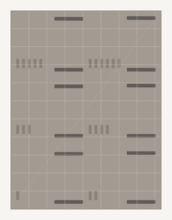
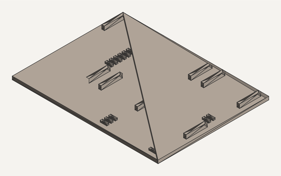
esp32-fit-gauge.stl: the flat top view, and an isometric projection of the
same mesh, both drawn from that file's bytes by
verify-stl.cjs
— renders, not photographs of a part. The isometric view is where you can see that the
walls stand up off one flat base and that every channel is open at both ends. What it
cannot show you is which channel is which: the step between neighbours is finer than this
drawing resolves at page size, so identify a channel by counting the ribs beside it, never
by eye off the picture.- Six U-channels: 24.6, 25.0, 25.4, 25.8, 26.2 and 26.6 mm. A
0.4 mm step between neighbours, so a reading is good to that step and no better.
That band is the one published as an STL above, chosen to straddle the
board this page is about.
fitGauge()inmodels.cjstakes an optionalcentre, so the generator will hand you the same six channels and the same step re-centred on a rough width you supply for some other board — a file you build locally, and one that asserts nothing about that board either. Your estimate only decides where the ladder sits; the board still does the talking. - How you read it. Lower the board into each channel from above. The narrowest channel it settles into without being forced is the one to report.
- Rib count identifies the channel. One rib beside the narrowest, six beside the widest; ribs are 1.6 mm wide on a 3.2 mm pitch, 5.0 mm long and 1.2 mm tall. The count survives you putting the part down and picking it up again, which a printed-on label at this size would not.
- Channels are 16 mm long and open at both ends, so you engage a short section of bare PCB edge instead of fighting the pin headers.
- Laid out two across and three down rather than in a line. In a single row the same six channels come to a 213 mm strip, which only just clears a 220 mm bed and wastes most of the plate.
The jumper-wire comb
Concede the obvious first: if what you want is a finished jumper-wire comb, the model repositories have thousands of them, and searching for one is not hard. This one has not been printed by anybody. If a file to send straight to a slicer is the whole job, go and take one of theirs; it is a better answer to that question than this is.
What page one of that search does not hand you is this surface: the number that sets the part, the STL, the source that built it, and a drawing made by a reader that shares no code with the writer, all published beside each other. That is the only thing this page adds. The comb is here because a second part makes that surface worth more than one part did — the same generator, the same checks, a different shape.
jumper-wire-comb.stl — 84.01 × 9.08 × 5.6 mm overall, 396 triangles, 19884 bytes. A flat bar with 32 teeth standing on it, leaving 31 slots. Press a wire into each slot and the bundle comes out spaced the way the holes are spaced.
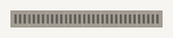
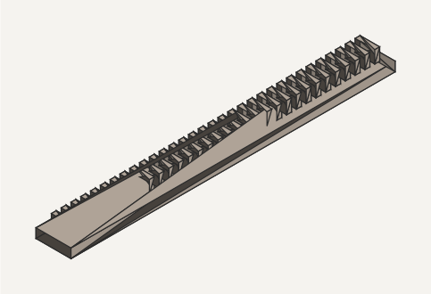
jumper-wire-comb.stl: the flat top view and an isometric projection, both
written by
verify-stl.cjs
out of the finished bytes it had just parsed back off disk. Renders, not photographs
— nothing here has been printed. At page size the drawing cannot resolve a
1.27 mm slot from a 1.27 mm tooth, so read the spacing off the numbers below
rather than off the picture.Where the 2.54 mm comes from
Every dimension of this part descends from one published figure: 2.54 mm, which is 0.1 inch exactly — the through-hole lead spacing that DIP packages, 0.1” pin headers and solderless breadboard tie-points are all laid out on.
That is the same pitch this page already cites two sections up as the reason a half-size (BB400) footprint can be stated at all without measuring anybody's breadboard: the 83.5 × 54.5 mm outline follows from the grid, not from a vendor's tooling. It is a defined conversion, not a measurement, so it is the one number on this page that cannot be wrong.
From it, without touching a caliper:
- Tooth centres 2.54 mm apart. That is the entire point of the part:
wires held in adjacent slots leave the comb at the spacing of adjacent tie-point columns.
test-fit.cjsmeasures the centres off the finished solids, andverify-stl.cjsre-derives them a second time from float32 vertices that have been through the STL encoder and back, because a generator asserting a pitch about its own variables proves nothing. - Teeth and slots each 1.27 mm — half the pitch. One tooth plus one slot has to add up to 2.54 mm, so the split is the only real choice, and an even one is the widest slot you can cut before the tooth becomes the thinner of the two members. No fact about any wire went into it, which is the point. See the limit below.
- Teeth 5.08 mm deep — two pitches — and 3.2 mm tall on a 2.4 mm base, reusing the plate's own wall height and base thickness rather than introducing new ones. Overall height is 5.6 mm, the same as the plate.
- 32 teeth, and that count is derived too. Called with no argument,
jumperComb()returns the longest comb that still lies inside the 84.1 mm breadboard bay of the plate at the top of this page: 32 teeth comes to 84.01 mm. Ask for 33 and the generator throws rather than quietly handing you a comb that will not sit in the part it was sized against.
The limit, stated plainly. A 1.27 mm slot is a geometric consequence of the pitch, not a measurement of anything you own. Nothing here has measured the jacket of a jumper wire, and a wire whose insulation is fatter than 1.27 mm will not enter the slot. That is the one thing worth checking against your own wire before you spend filament, and it is the sort of check this page cannot do for you, because this page has no wire and no printer.
The tooth count is a control in this tab. If the comb above is the wrong
length for what you are doing, type the count you want into
Build a comb with the number of teeth you want, further down this
page, and the same jumperComb({ teeth }) in
models.cjs runs in your
browser instead of on your machine. Running build.cjs yourself does the same thing
and is still there if you would rather.
Which numbers are asserted, and which are not
Provenance table: where each number in models.cjs came from — 13 rows, a header plus one row per parameter, including the two still marked UNVERIFIED
| Parameter | Status |
|---|---|
| Breadboard footprint, 83.5 × 54.5 mm | Standard BB400 half-size footprint, fixed by 2.54 mm pitch. Bay span asserted by test-fit.cjs. |
| Breadboard clearance, 0.6 mm | Design choice. Asserted only in the sense that the bay is neither undersized nor sloppy. |
| Devkit board width | UNVERIFIED in models.cjs — a placeholder, never sourced, never measured. This page does not restate it as a fact about the board. It is the number the gauge exists to measure. |
| Devkit board length | UNVERIFIED in models.cjs. Made harmless by leaving the bay open at both ends — test-fit.cjs asserts that openness directly. |
| Devkit clearance, 0.8 mm | Design choice. The intent is that a full millimetre of error in the unverified width would still leave the bay usable; nothing has tested that, because nothing has been printed. |
| Devkit bay, 26.2 mm | Follows arithmetically from an UNVERIFIED input, so treat it as a guess with a margin. The finished span is asserted by test-fit.cjs; what it is a good span for is not. |
| Six channel widths, 24.6–26.6 mm | Asserted: test-fit.cjs measures each finished channel against its stated width. |
| Base 2.4 mm, walls 2.0 mm × 3.2 mm, notches 12.0 mm | Design choices, read straight from the parameter block. |
| Tie-point pitch, 2.54 mm | A published standard, and a defined conversion: 0.1 inch exactly, the through-hole lead spacing DIP packages, 0.1” headers and breadboard tie-points share. Not measured here, and not measurable wrongly. |
| Comb teeth and slots, 1.27 mm each | Half the pitch, by arithmetic. Asserted: test-fit.cjs scans each finished slot, and verify-stl.cjs re-measures the tooth faces from the encoded bytes. NOT asserted: that any particular jumper wire fits a 1.27 mm slot. No wire has been measured. |
| Comb tooth count, 32 | Derived: the largest count whose overall length (84.01 mm) still lies inside the plate's 84.1 mm breadboard bay. Asserted by test-fit.cjs against the plate's own bay, not against a literal. |
| Comb tooth depth 5.08 mm, height 3.2 mm, base 2.4 mm | Two pitches, and the plate's own wall height and base thickness reused. Design choices with no hardware input. |
What the checks actually check — all 26 assertions in full, and why the plate mesh has four four-triangle edges (about 1,100 words)
What the checks actually check
node tools/print/test-fit.cjs takes a scan line across the finished solids at
wall height and reports the clear span, the way a caliper would, rather than trusting the
arithmetic that produced them. Twenty-six assertions pass:
bench plate
  ok   the breadboard bay is wide enough for a BB400, and not sloppy
  ok   the breadboard bay is DEEP enough, and not sloppy
  ok   the devkit bay holds the board width with the intended clearance
  ok   the devkit bay is OPEN end to end, so an unverified board LENGTH cannot bind
  ok   the rear wall really is notched for cables
  ok   nothing overhangs: every solid sits on the base or on another solid

fit gauge
  ok   every channel measures its stated width
  ok   the ribs never intrude into a channel
  ok   channel widths bracket the nominal 25.4 mm guess in both directions
  ok   the PUBLISHED band is exactly the array the STL on the site was built from

fit gauge, re-centred on a supplied width
  ok   a supplied centre is bracketed in both directions
  ok   the re-centred ladder keeps the 0.4 mm default step, evenly spaced
  ok   every re-centred channel measures its stated width, and no rib intrudes
  ok   the re-centred solid is still a valid, non-interpenetrating mesh
  ok   a re-centred gauge does not disturb the default one

jumper-wire comb
  ok   the teeth stand on exact 2.54 mm tie-point centres
  ok   every slot between two teeth is exactly half the pitch wide
  ok   the teeth are as thick as the slots, so neither member is the weak one
  ok   the default comb lies inside the breadboard bay of the plate on the same page
  ok   bounds() agrees with the meta the generator reported
  ok   nothing overhangs: every tooth stands on the base
  ok   the mesh is valid and no two solids interpenetrate

jumper-wire comb, at a tooth count the caller chose
  ok   a shorter comb keeps the pitch and stays a valid mesh
  ok   the overall size is the tooth count and the pitch, and nothing else
  ok   counts that cannot work are refused, not quietly built
  ok   a comb of another length does not disturb the published one

26 assertion(s) passed
That third assertion is worth reading carefully. It checks the bay against the parameter, not against a real board — it confirms the generator did what the parameter block asked for, which is a different and much weaker claim than "your board will fit". The same measurement pass earned its keep during design: a stray 4 mm term had inflated the devkit bay to 30.2 mm, four millimetres of slop that the arithmetic hid and the scan line caught.
node tools/print/verify-stl.cjs then re-reads the bytes that actually landed on
disk with a separate parser, on the principle that a generator validating its own memory says
nothing about the file. Run against the three STLs this page serves, it reports 408 triangles
for the gauge, 396 for the comb and 96 for the plate, all three sitting exactly on Z=0, with
every facet normal agreeing with its winding order.
All six preview images above are that tool's own output — one flat top view and one isometric projection per solid, written to disk in the same pass that did the re-reading — not drawings made by hand.
Every edge, counted. That same pass now also tallies undirected edges: for each edge of each triangle it parsed, it counts how many triangles use that same line. On one closed surface the answer is exactly two, everywhere — an edge used once is a hole in the shell, and an edge used more than twice is several sheets meeting along one line.
The gauge (408 triangles, 612 distinct edges) and the comb (396 triangles, 594 edges) both come back with zero edges that are anything other than twice-used: they are closed meshes. The plate (96 triangles, 140 edges) comes back with zero edges used once and four edges used by four triangles each, so the plate is not one closed surface.
The tool prints that number for every file it reads; it does not assert it, because the number is a property of how the part is built rather than a fault that crept in.
The four build controls further down print the same tally for the part you build, counted the same way out of the same bytes they hand you — and the tray is the one part on this page whose boxes were laid out so that the answer is always zero and zero, which its own section explains.
Why four, and where. The writer in
stl.cjs has no boolean
operations. A part is a set of axis-aligned boxes that touch but never share volume — a recess
here is four walls standing on a slab, not a hole cut out of one — and nothing ever unions
those boxes into a single skin.
So wherever two wall boxes meet at a shared corner, the vertical line at that corner is a genuine edge of both boxes, and each box contributes two triangles to it: four in total. The plate has exactly four such corners — two where the left-hand side wall butts into the front and rear walls, and two where the bay divider does the same.
Each of the four lines runs the 3.2 mm wall height, from the top of the
2.4 mm base to the top of the wall, and verify-stl.cjs prints all four sets
of coordinates. The gauge and the comb score zero because no two of their boxes ever share an
edge line: their solids stand on the base without meeting each other end-on.
What you may see, and what has not been established. A program that inspects meshes when you open a file can be expected to notice this and offer to repair it, and coincident contacts between solids that are meant to be one part are the ordinary case such repairs exist for — so the expectation is that it is handled.
That is an expectation, not a measurement: nothing here has tested any particular program, and none is named. No repair has been applied to the file either — the bytes you download are the bytes the generator wrote, four-triangle edges and all.
Rearranging the boxes does not remove them: with the walls turned so the long sides run the full depth and the end walls sit between them, the count is still four, and giving each corner its own post makes it sixteen. Removing them properly means a boolean union, which this kernel does not have. And nothing on this page has been printed, so this says nothing about how the plate prints.
Downloads
- esp32-bench-plate.stl (4884 bytes) · top-view preview (SVG) · isometric preview (SVG)
- esp32-fit-gauge.stl (20484 bytes) · top-view preview (SVG) · isometric preview (SVG)
- jumper-wire-comb.stl (19884 bytes) · top-view preview (SVG) · isometric preview (SVG)
All three are binary STL in millimetres, sitting on Z=0, so they import at the right scale and orientation with nothing to rotate or rescale. That is a statement about placement, not about the mesh: as the edge count above records, the gauge and the comb are closed meshes and the plate is not, so a program that inspects meshes on import may flag the plate and offer to repair it. They are served from this site — the same bytes the repository holds, not a re-export from somewhere else.
The source files this page describes
The five files below — served as plain text — are the entry point that produced the three STLs on this page, the generator it takes its geometry from, the binary-STL writer it requires, and the two checkers that measured the finished solids and re-read the written bytes.
build.cjs is the entry point that ties the other four together: it builds all
three solids, runs the mesh check on each, and writes that part's .stl only if the
check passed — a part whose check fails prints its problems and leaves no file behind. Read
the check narrowly: it says the solids making up a part do not interpenetrate and that the
file was written only because that held, and it says nothing about whether the part fits a
board, prints cleanly, or is the right shape.
The thinking behind these five files is written up at Generating 3D-Printable Parts From Code — why the kernel has no boolean operations, so a recess here is four walls standing on a plate rather than a hole cut into a block, and the defects that surfaced on both sides of the checks.
Printing them
All three of the files above have a flat bottom, nothing overhangs, and the tallest feature on any of them is 5.6 mm, so as guidance: lay them on the bed as they arrive, and you should not need supports, a raft or a brim. PLA is fine — none of them carries load or heat. 0.2 mm layers, three perimeters and light infill are plenty; these are bench furniture, not machine parts, and there is nothing to gain from a slow profile.
The tray you can build further down is the same in kind and taller: its walls stand straight up off a flat floor, so nothing overhangs there either, but it is 14.4 mm tall rather than 5.6 mm whatever size you ask for, and above the floor it is nothing but wall.
Those are statements about the shape the generator emits, and that is all they are: no version of the tray has been sliced, printed, timed or weighed, so this page has no print advice for it beyond what it has for the others.
The repository README puts the gauge at roughly fifteen minutes. Treat that as a rough estimate with no slicer behind it and no printer behind it either — slice the file and believe your own number.
Print the gauge first. It is the smaller part and it is the one that turns the unverified width parameter into a measured one, after which the generator emits a plate sized to the board rather than to a guess.
Make a plate sized to the numbers you measured — the in-browser generator: one width box, two optional breadboard boxes (about 830 words)
Make a plate sized to the numbers you measured
The gauge exists to replace a guess with a number. This is where the number goes: type the width of the narrowest channel your board settled into without forcing, and the plate is rebuilt around that figure and handed to you as a binary STL.
Only the devkit bay moves with that number — and, with it, the overall plate width. The base and wall thicknesses are untouched, because nothing the gauge measures affects them. The breadboard bay keeps the footprint the generator already carries unless you measure your own breadboard into the two boxes below; give it a length and a width and that bay, the plate's depth and the two cable notches spaced along it all move with your numbers instead.
This is not a second implementation of the geometry, which is the usual way a browser
version of a part quietly stops matching the real one. The module the button runs,
geometry.js, is generated
verbatim from the same models.cjs
and stl.cjs listed above,
by tools/print/make-web-geometry.cjs.
A test in the repository re-runs that
generator and fails if the served copy differs by a single byte, and separately builds the
plate at the file's own parameters and requires the result to be byte-identical to the
esp32-bench-plate.stl this page serves. The browser and the command line are the
same code path, and that is checked rather than claimed.
Everything happens in this tab. The number is read from the box below, used to build an array of bytes in memory, and handed to the browser as a download; it is not sent anywhere, not stored, and no request is made in order to build it.
Before a link appears, the module runs
the two functions the command-line build gates on — check(), which rejects
degenerate triangles and any pair of solids that share volume, and bounds(), which
measures the finished triangles instead of trusting the arithmetic that produced them. If
either comes back wrong you get the reason in plain words and no file, the same way
build.cjs leaves no file behind when a check fails.
Your own breadboard, if it is not the one the generator was written
around. The plate has two bays, and until now only one of them was yours: the
breadboard bay is built from a footprint fixed in
models.cjs, so a
solderless breadboard of some other size had nowhere to go. These two boxes take its outer
length and its outer width off your own ruler, the same way the box above takes your board.
- Leave both empty and nothing changes: the bay is built from the figure already in the generator, under the filename this control has always used.
- Fill both and the bay is built from your two numbers, which are written into the filename so two plates cannot be confused on disk.
- Fill one and leave the other empty and you get a refusal instead of a file, because a bay needs both of its dimensions and half a measurement is a guess.
A plate you generate here has not been printed either. It is the same kind of object as the three files above: geometry a computer has checked and a printer has never seen. The generator built the mesh to the number you typed and verified that mesh. What nobody did is print it, put a board in it, or measure the result. If your reading of the gauge is off, the part is off by the same amount, and nothing on this page can tell you so.
Re-centre the gauge on a number you already have — the in-browser generator: one box for a rough width (about 400 words)
Re-centre the gauge on a number you already have
The gauge this page serves as a file brackets a width that came from the generator's placeholder, which is only useful if the board you are measuring happens to sit near it.
If you already have a rough figure — a caliper reading you do not trust to a tenth, a dimension you took off a DXF yourself in a CAD viewer, or the fact that a previous reading landed hard against one end of the published ladder rather than in the middle — type that figure below.
The channels are rebuilt centred on it, keeping the same step between them and the same rib groups counting up so a channel can be told apart from its neighbours without a label. Nothing else about the part changes. The depth does follow the number you ask for, because the rows have to be pitched far enough apart for the widest channel, and the control reports the envelope it measured before it offers you anything.
It runs the same ladder of checks as the plate control above, in the same order, and refuses in the same way.
It has one refusal the plate control does not need: ask for a centre low enough and the bottom of the ladder reaches zero width, which is a part with no channel in it. The mesh check does not object to that — a zero-width channel is still a closed set of triangles — so the module reads the built channel widths back and tells you what the narrowest one came out at instead of handing you the file.
A re-centred gauge has not been printed either. No version of it has. It is the same kind of object as everything else here: a mesh a computer built to the number you gave it and then checked. Whether it tells you anything useful depends entirely on whether the figure you typed was close enough to be worth bracketing, and nothing on this page can tell you that.
Build a comb with the number of teeth you want — the in-browser generator: tooth count is its only parameter (about 560 words)
Build a comb with the number of teeth you want
Length is the comb's only parameter. The file this page serves is as long as the generator will go, because the count was derived by asking how many teeth still fit inside the breadboard bay of the plate at the top of the page — a sensible thing to derive it from, and a completely arbitrary answer to the different question of how many wires you are trying to keep in order.
If you want a short one to sit at the edge of a project box, or a stub to hold the four wires of an I²C run, the number is yours to pick. Type it below and the comb is rebuilt at that count and handed to you as a binary STL.
Only the count changes. The pitch, the tooth and slot widths, the tooth depth, the base and the wall height are all fixed — they come from the plate's own parameters and from the breadboard pitch, and none of them is a function of how many teeth you ask for.
So a comb you build here is the published one made shorter, not a differently proportioned part. The control reports the widths it actually built, read back out of the generator's output, so you can see that for yourself rather than take this paragraph's word for it.
The refusals are the generator's, not this page's. jumperComb() already throws,
with a written reason, for a count that is not a whole number, for one below the shortest comb
it makes, and for one longer than the bay allows.
The module catches that error and prints its message verbatim, in quotation marks, instead of restating it — which means the ceiling you are told about is the one the function computed, and this page cannot drift away from it.
Past that, a comb runs the same ladder of checks as the plate and gauge controls above, in the same order:
check()for degenerate triangles and solids sharing volume,bounds()re-measured off the finished triangles and compared against the width, depth and height the generator said it was making,- the part sitting on Z=0,
- and the
finished file's byte length coming out at exactly what binary STL's fixed header and fixed
per-triangle record add up to for the triangle count
check()reported.
Any one of those failing means a reason and no file.
A comb you generate here has not been printed either. None of them has. And the one thing worth checking before you print — whether the jacket of your wire will enter a slot — does not change with the tooth count, because the slot width is half the pitch at every count. Nothing here has measured a wire. A shorter comb is a shorter comb; it is not a comb that answers a question this page cannot answer.
Build a tray for the loose parts on your bench — the in-browser generator: inside length and inside width, both required (about 860 words)
Build a tray for the loose parts on your bench
An open-top rectangular box, sized from the two numbers that actually matter about a tray:
how long the hole in the middle of it is, and how wide. Everything else is fixed — a
2.4 mm floor and 2 mm walls, both taken from the bench plate at the top of this page
rather than picked again, and a 12 mm wall height that was simply chosen and is labelled
as a choice in
models.cjs. Nothing
has been measured against that 12 mm: not a header strip, not a screw, not a jumper end.
Why there is no bench-tray.stl to download. The other three
parts have a published size because something outside this repository fixes it: the breadboard
footprint follows from 2.54 mm tie-point pitch, the gauge's ladder brackets a board width,
the comb's tooth count is the longest that still sits in the plate's bay.
A tray has no such
anchor. How much loose hardware is on your bench, and how much room you have to put it, are
facts about your bench, and this page's whole rule is that it does not invent those. So
benchTray() ships with no default size at all: call it without both inside
dimensions and it throws, and the control below prints that refusal in the generator's own
words instead of quietly building something.
It is generated and checked, and that is the entire claim. No tray has been printed, test-fitted, filled, or held up against a real part.
What happens when you press the button is that geometry is built from your two numbers and then examined by code, in front of you:
check()for degenerate triangles and for any pair of solids sharing volume,bounds()re-measured off the finished triangles and compared with the width, depth and height the generator said it was making,- the part sitting on Z=0,
- and the file's byte length
matching what binary STL's fixed header and per-triangle record add up to for the triangle count
check()reported.
There is one check no other control on this page runs: the
built solids are compared against the cavity the generator says it left, on all three axes at
once, so a wall standing in the middle of the hole would be caught. check() has no
opinion about that — material in the wrong place is still a sound mesh.
The corners are stepped on purpose, and the edge tally is how you can tell. As the edge count above records, the bench plate is not one closed surface: wherever two of its wall boxes meet at a shared corner, the vertical line at that corner is a real edge of both boxes and four triangles land on it.
The tray is laid out so that never happens. Its two end walls run the full width of the base; its two side walls sit between them, inset by the same 2 mm margin the plate uses, so each side wall lands on a face strictly wider than itself — a T-junction rather than a butt joint — and shares no vertex with it.
Five boxes, sixty triangles, ninety distinct edges, none of them shared — so every tray this control builds comes back zero used once, zero used more than twice, at every pair of dimensions. That costs something you can see on the part: a 2 mm ledge of bare base right round the outside, and end walls that stand 2 mm further out at each side than the side walls do.
Both are real, not rendering artefacts, and both show up in the top view the control draws. You do not have to take any of this on trust: the tally printed under your download is counted out of the bytes you were just handed, by a parser that has never seen the generator.
A tray you build here has not been printed. None has. Whether 12 mm is deep enough for what you want to put in it, whether the walls are stiff enough at 2 mm, and whether a 200 mm tray fits your bed are all questions this page cannot answer, because it has no printer, no filament and no bench. What it can tell you is that the geometry closes and that the hole is the size you asked for, and it shows you the count both times.
What this page does not claim
- That any part on this page fits anything — the three files above or the tray built in your browser. Nobody has put a board in one, nobody has put a wire in the comb, and nobody has put a screw in the tray.
- Any tolerance, surface finish, stiffness or material result. None was measured.
- Any print time observed on a printer. None was observed.
- That anyone has downloaded, printed or used these files.
- That any particular program will repair the plate's four four-triangle edges when you open it. That is stated above as an expectation and nothing more; no program was run against the file here, and none is named.
- That a plate generated in your browser will fit your board. The generator built the geometry to the number you gave it and checked the mesh; that is the whole of it.
- That a gauge re-centred in your browser will read anything usefully. Its channels were built around the figure you typed and the mesh was checked; nobody has printed one or put a board in it.
- That a comb built to your own tooth count will hold your wires. The generator made a comb that long and the mesh was checked; the slot width is a consequence of the pitch at every count, and no wire has been measured against it.
- That a tray built in your browser will hold what you want to put in it, or that 12 mm is a sensible depth for anything. Both of those are the same kind of claim: untested. The generator left a hole of the two sizes you typed and the code checked that the hole is empty and that the surface closes around it. Nothing else about it is known here.